
TechSkills of Future

Computer processors-CPUs: Working, architecture and Diagram

Processor Architecture – Digital Electronics
ALU CTRL REGISTERS CACHE

Introduction to
Processor Architecture

“Complex Logic. Simple Execution-CPUs–> The Heart of Every Computer.”
// Single Cycle · Multicycle · Pipelined
CPU DESIGN DATAPATH PIPELINE MICROARCHITECTURE

A Simple Computer

The foundation of modern computing: CPU connected to memory via address and data buses, orchestrating the fetch-decode-execute cycle.

CPU Instruction Decoder CONTROL Registers ALU Program Counter (PC) + Adder ADDRESS BUS DATA BUS MEMORY 0x0000 0x0001 0x0002 0x0003 0x0004 0x0005 10110010 01001101 11100001 00110100 10010110 01101011
FIG 1 — COMPLETE SIMPLE COMPUTER ARCHITECTURE
????️
CPU
Central Processing Unit with Instruction Decoder, Registers, ALU, and Control Unit working in concert.
????
Memory (RAM)
Stores both instructions and data. Word-addressable — each address holds a full 32-bit word.
Buses
Address bus (CPU→Memory) carries location to read/write. Data bus (bidirectional) carries the values.

MicroArchitecture

Architecture defines what the processor does. Microarchitecture defines how it’s built — the specific arrangement of hardware to implement it.

Architecture vs Microarchitecture

A computer architecture is defined by its instruction set and architectural state. For example, the MIPS architecture’s state comprises:

Program Counter (PC) 32 General Registers

The microarchitecture is the hardware implementation — registers, ALUs, FSMs, multiplexers, and memory — arranged to execute that architecture. One architecture can have many microarchitectures with different trade-offs.

Two Key Parts

????
Datapath
Operates on data words (16/32-bit). Contains memories, registers, ALUs, multiplexers. The PC is a register whose output points to the current instruction.
????️
Control Unit
Receives instructions from the datapath and issues mux select signals, register enables, and memory write signals to drive the datapath.
DATAPATH CONTROL UNIT PC Reg Instr. Memory Register File R0 — R31 32-bit each ALU MUX Data Mem Instruction Decoder / FSM Control generates: RegEnable · MuxSel · MemWrite · ALUOp receives: opcode · func fields · flags
FIG 2 — MICROARCHITECTURE COMPONENTS

Building a Single-Cycle CPU

We incrementally build the datapath — starting with pure instruction fetch, then adding branching, register operations, memory access, and finally branching control.

1

Fetch Instructions

Program Counter Instr. Memory +1 Addr Instruction PC+1 1
PC → Memory address → Instruction fetched → PC + 1
  • ✦ PC supplies address to instruction memory
  • ✦ Memory outputs instruction to datapath
  • ✦ Adder increments PC by 1 each cycle
  • ✦ Limitation: no branching, no data access
2

Register Access + ALU

Machine Instruction Format

OP opcode rd destination rs1 source 1 rs2 source 2
; ADD R1, R2, R3 → R1 = R2 + R3 OP rd rs1 rs2 010 001 010 011 ; op=ADD rd=R1 rs1=R2 rs2=R3
Instr. Decoder rs1 rs2 rd function (ALU op) Register File R0..R7 32-bit ALU Result → rd zero
3

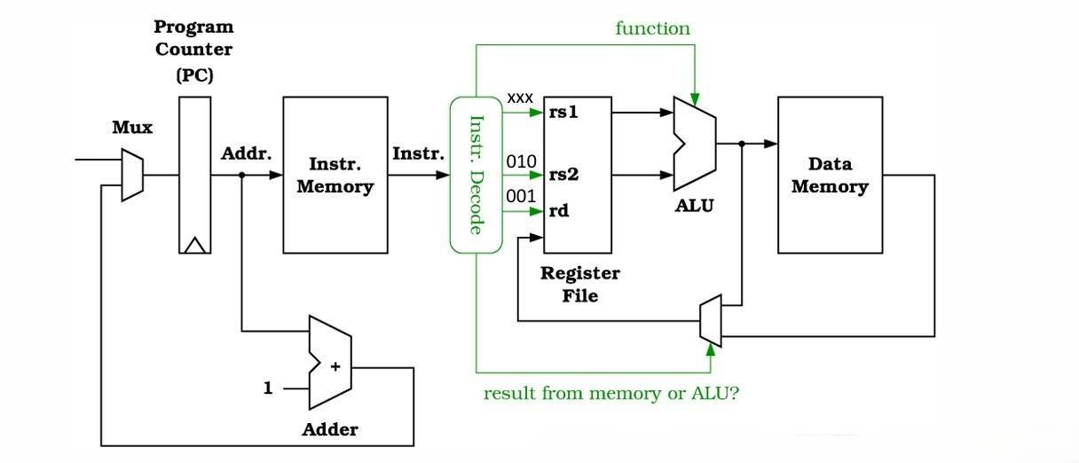
Memory Access — LOAD/STORE

LOAD R1, [R2] ; R1 = MEM[R2] — load from address in R2 STORE R1, [R2] ; MEM[R2] = R1 — write R1 to address in R2

Building a simple computer –memory access
https://tecxskill.com/computer-processors-cpus-working-architecture-and-diagram/

.

A MUX selects whether the register file receives its write data from the ALU result or from the Data Memory output — enabling both arithmetic results and memory loads to be stored back to registers.
4

Branching — BEQZ

BEQZ R1, +10 ; if (R1 == 0) then PC = PC + 10 ; Branch if Equal to Zero — conditional jump
PC MUX Instr. Memory +1 +offset AND branch? zero? MUX sel R1 value
  • ✦ ALU checks if R1 is zero → zero flag
  • ✦ Decoder signals: branch = 1
  • ✦ AND gate: branch AND zero
  • ✦ If true → MUX selects jump adder output
  • ✦ Jump adder: PC + offset (+10)
  • ✦ If false → normal PC+1 path
The MUX at the PC input is the key — it chooses between sequential execution and a branch target, controlled by the AND of the branch signal and the zero flag.

Three Processor Designs

From single-cycle through multicycle to pipelined — each design trades complexity for performance in different ways.

Feature Single-Cycle Multicycle Pipelined
Clock Period Fixed — slowest instruction Shorter — per step Shortest — 1 stage
Adders Needed 3 (ALU + 2 PC logic) 1 (reused) 2 (reused)
Memory Separate instr + data Shared single memory Separate (optimised)
Control Combinational logic FSM FSM + hazard unit
Throughput 1 instr / long cycle Variable steps ~1 instr / short cycle
Complexity Low Medium High
Hazards None None Data + Control hazards

Clock Cycle Timing Comparison

time → SINGLE CYCLE LONG Instruction SHORT Instruction LONG Instruction min period = LONGEST instr MULTI CYCLE S1 S2 S3 S4 S5 S1 S2 short done early! S1 S2 S3 S4 S5 min period = one SHORT step PIPELINE I1:IF I1:ID I1:EX I1:M I1:WB 5 instrs executing simultaneously → 5× throughput

⚡ Performance Equation

Time / Program = Instruction Count × CPI × Clock Period CPI = Clocks Per Instruction Clock Period = 1 / Frequency

Multicycle Processor

Break instructions into smaller, reusable steps. Simple instructions finish early; complex ones take longer. One memory, one adder — shared across cycles.

3 Weaknesses of Single-Cycle

  • ⚠ Clock must accommodate the slowest instruction every cycle
  • ⚠ Requires 3 adders — 1 in ALU, 2 in PC logic — all idle most of the time
  • ⚠ Needs separate instruction and data memories — expensive duplication

Multicycle Advantages

  • ✅ Shorter clock period = only 1 step’s worth
  • ✅ ALU reused across multiple steps in one instruction
  • ✅ Single shared memory — instruction fetched in step 1, data in later steps
  • ✅ Simple instructions complete faster than complex ones

Instruction Execution Steps (FSM States)

STEP 1
Fetch
IF
STEP 2
Decode
ID
STEP 3
Execute
EX
STEP 4
Mem R/W
MEM
STEP 5
WriteBack
WB
Non-architectural state registers hold intermediate results between steps:
IR (Instruction Reg) MDR (Mem Data Reg) A, B (ALU inputs) ALUOut

FSM Control — State Transitions

FETCH S0 DECODE S1 EXEC S2-ALU MEM S2-MEM WRITE BACK always ALU instr LOAD/STORE result mem done → Fetch next

Pipelined Processor

Divide instruction execution into 5 stages. While one instruction is in stage 2, another enters stage 1. Ideal throughput: 1 instruction per clock cycle.

5-Stage Pipeline

IF
Instruction
Fetch
ID
Decode &
Reg Fetch
EX
Execute
ALU
MEM
Memory
Read/Write
WB
Write
Back

Instructions in Flight

Instr T1 T2 T3 T4 T5 T6 T7 T8 T9 I1 IF ID EX MEM WB I2 IF ID EX MEM WB I3 IF ID EX MEM WB I4 IF ID EX MEM WB I5 IF ID EX MEM WB all 5 stages full

⚠ Pipeline Hazards

Data Hazard

An instruction tries to read a register that a preceding instruction hasn’t finished writing to yet.

; Hazard example: ADD R3, R1, R2 ; writes R3 SUB R4, R3, R5 ; reads R3 TOO EARLY!
Solutions: Forwarding (bypass units), stall/bubble insertion, out-of-order execution

Control Hazard

When a branch instruction is in the pipeline, we don’t yet know which instruction to fetch next — but we have to fetch something.

; Branch hazard: BEQZ R1, +10 ; branch? ADD R2, … ; fetched, but wrong?
Solutions: Branch prediction, delayed branching, flush on misprediction
Register File write-then-read: In a pipelined processor the register file is written in the first half of a clock cycle and read in the second half, allowing a write and read of the same register to occur within a single cycle — reducing data hazard stalls.

Key Concepts

Instruction Set Reference

Instruction Syntax Operation Type
ADD ADD rd, rs1, rs2 rd = rs1 + rs2 ALU
SUB SUB rd, rs1, rs2 rd = rs1 − rs2 ALU
LOAD LOAD rd, [rs2] rd = MEM[rs2] MEM
STORE STORE rs1, [rs2] MEM[rs2] = rs1 MEM
BEQZ BEQZ rs, offset if(rs==0) PC=PC+offset BRANCH
JUMP JUMP target PC = target (unconditional) JUMP

Component Glossary

⚙️
ALU
Arithmetic Logic Unit — performs ADD, SUB, AND, OR, comparisons. Sets zero/carry/overflow flags.
????
Register File
Small, fast storage inside CPU. Typically 8–32 registers of 32-bit width. 2 read ports, 1 write port.
????
Multiplexer (MUX)
Selects one of N inputs to pass to output based on control signal. Critical for routing datapath.
????
FSM
Finite State Machine. Controls multicycle and pipelined processors — produces outputs based on state + inputs.
????
Program Counter
Register holding address of next instruction. Incremented by 1 each cycle (or updated by branch/jump).
????
Zero Flag
ALU output flag set when result = 0. Used by BEQZ to decide whether to branch.
IDEAL PIPELINE SPEEDUP
(5-stage)
32
TYPICAL REGISTER COUNT
(MIPS / RISC-V)
1
INSTRUCTION PER CYCLE
(IDEAL THROUGHPUT)

Additional Important Points

????
RISC vs CISC
RISC (Reduced Instruction Set) = simple, fixed-length instructions, easy to pipeline. CISC (x86) = complex variable-length instructions, harder to pipeline, uses microcode internally.
⏹️
Cache Hierarchy
L1 (fastest, smallest, on-chip) → L2 → L3 → RAM. Pipelined CPUs split L1 into Instruction Cache (I$) and Data Cache (D$) to allow simultaneous IF and MEM stages.
⏱️
Amdahl’s Law
The speedup of a system is limited by the fraction that can’t be parallelised. Pipeline stages that must stall limit overall throughput improvement.
????
Branch Prediction
Modern CPUs predict whether branches will be taken. A misprediction flushes the pipeline (costs ~15–20 cycles). Static (always not-taken) and dynamic (history-based) predictors exist.
????
Forwarding / Bypassing
Solve data hazards without stalls by routing the ALU output directly back to an earlier pipeline stage’s input — avoiding the wait for register writeback.
????️
Word Addressable Memory
Each memory address holds a full 32-bit word (not a single byte). Simplifies the datapath — address increment of +1 means “next instruction,” not “+4 bytes.”

Leave a Comment

Your email address will not be published. Required fields are marked *