
01 Binary ⇌ Gray Conversion Logic
Timing Waveform
Gray to Binary Logic Circuit
Gray to Binary (Loop Method)
module gray_to_binary #(parameter N=4) (
    input [N-1:0] gray,
    output reg [N-1:0] binary
);
    integer i;
    always @(*) begin
        binary[N-1] = gray[N-1];
        for (i = N-2; i >= 0; i = i - 1)
            binary[i] = binary[i+1] ^ gray[i];
    end
endmodule
Binary to Gray (Shift Method)
module binary_to_gray #(parameter N=4) (
    input [N-1:0] binary,
    output [N-1:0] gray
);
    assign gray = binary ^ (binary >> 1);
endmodule| Decimal | Binary | Gray |
|---|---|---|
| 0 | 0000 | 0000 |
| 2 | 0010 | 0011 |
| 5 | 0101 | 0111 |
| 7 | 0111 | 0100 |
02 Binary to Two’s Complement
Timing Waveform
Operation: $\text{Result} = \text{NOT}(\text{A}) + 1$. This converts a positive magnitude to its negative equivalent in signed systems.
Structural Logic
Truth Table (3-bit)
In: 001 (1)
In: 010 (2)
In: 100 (4)
In: 010 (2)
In: 100 (4)
Out: 111 (-1)
Out: 110 (-2)
Out: 100 (-4)
Out: 110 (-2)
Out: 100 (-4)
module twos_complement #(parameter N=4) (
    input [N-1:0] a,
    output [N-1:0] y
);
    // Method 1: Mathematical
    assign y = (~a) + 1'b1;

    /* Method 2: Behavioral
    always @(*) begin
        y = (~a) + 1;
    end */
endmodule
03 BCD to 7-Segment Decoder
Timing Waveform
Physical Segment Map
Simplified SOP
$a = \sum m(0, 2, 3, 5, 6, 7, 8, 9)$
$b = \sum m(0, 1, 2, 3, 4, 7, 8, 9)$
$e = \sum m(0, 2, 6, 8)$
| Digit | BCD | a b c d e f g |
|---|---|---|
| 0 | 0000 | 1 1 1 1 1 1 0 |
| 3 | 0011 | 1 1 1 1 0 0 1 |
| 7 | 0111 | 1 1 1 0 0 0 0 |
module bcd_to_7seg(
input [3:0] bcd,
output reg [6:0] seg // {a,b,c,d,e,f,g}
);
always @(*) begin
case(bcd)
4'h0: seg = 7'b1111110;
4'h1: seg = 7'b0110000;
4'h2: seg = 7'b1101101;
4'h3: seg = 7'b1111001;
4'h4: seg = 7'b0110011;
4'h5: seg = 7'b1011011;
4'h6: seg = 7'b1011111;
4'h7: seg = 7'b1110000;
4'h8: seg = 7'b1111111;
4'h9: seg = 7'b1111011;
default: seg = 7'b0000000;
endcase
end
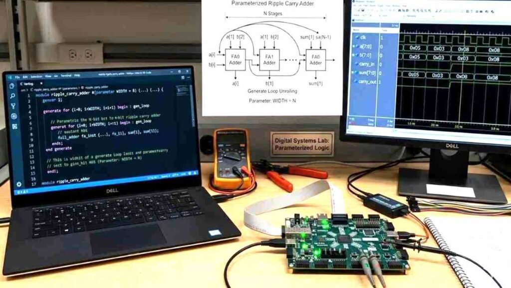
endmoduleAdvanced: Parameterized Ripple Carry Adder
Timing Waveform
Logic Schematic (Slice)
Verilog Hardware Generation
module ripple_carry_adder #(parameter WIDTH = 8) (
    input [WIDTH-1:0] a, b,
    input cin,
    output [WIDTH-1:0] sum,
    output cout
);
    wire [WIDTH:0] carry;
    assign carry[0] = cin;
    assign cout = carry[WIDTH];

    genvar i;
    generate
        for (i=0; i < WIDTH; i=i+1) begin : fa_inst
            full_adder fa (
                .a(a[i]), .b(b[i]), .ci(carry[i]),
                .s(sum[i]), .co(carry[i+1])
            );
        end
    endgenerate
endmodule
Verification & Timing
- For N=32, propagation delay involves 32 stages.
- Best for low-speed, area-constrained designs.
| A | B | Cin | Sum | Cout |
|---|---|---|---|---|
| 1010 | 0110 | 0 | 0000 | 1 |
| 1111 | 0001 | 0 | 0000 | 1 |
05 BCD to Excess-3 Logic
Timing Waveform
Verilog Design
module bcd_to_excess3(
    input [3:0] bcd,
    output [3:0] excess3
);
    // Continuous assignment for simple arithmetic
    assign excess3 = bcd + 4'b0011;
endmodule
Truth Table
BCD (In) -> XS3 (Out)
0000 -> 0011
0100 -> 0111
1001 -> 1100
Logic Diagram (Gate Level)
Functional Verification Results
Consolidated Simulation Output
GRAY CONV
T=10ns | B=0110 -> G=0101
T=20ns | G=1100 -> B=1011
T=30ns | B=1010 -> G=1111
T=10ns | B=0110 -> G=0101
T=20ns | G=1100 -> B=1011
T=30ns | B=1010 -> G=1111
7-SEGMENT
BCD: 0 -> SEG: 1111110
BCD: 5 -> SEG: 1011011
BCD: 9 -> SEG: 1111011
BCD: 0 -> SEG: 1111110
BCD: 5 -> SEG: 1011011
BCD: 9 -> SEG: 1111011
PARAMETER RCA
W=4 | A=F, B=1 -> S=0, C=1
W=8 | A=AA, B=55 -> S=FF, C=0
W=4 | A=F, B=1 -> S=0, C=1
W=8 | A=AA, B=55 -> S=FF, C=0
EXCESS-3
IN: 0000 -> OUT: 0011
IN: 1000 -> OUT: 1011
IN: 0101 -> OUT: 1000
IN: 0000 -> OUT: 0011
IN: 1000 -> OUT: 1011
IN: 0101 -> OUT: 1000