Microwave Discrete and Microstrip Filter Design
Theory, Design Methodology, Microwave filters are two-port networks that select desired frequency bands (passband) and suppress unwanted frequency bands (stopband). They are essential for signal clarity in commercial (5G, satellite) and military (radar) systems
1. Introduction
Modern RF and microwave systems such as wireless communication links, radar, satellite payloads, and sensing platforms require high-performance filters to ensure spectral purity and system stability. Unlike low-frequency filters, microwave filters must account for distributed effects, discontinuities, and electromagnetic coupling. Therefore, their design combines circuit theory, transmission-line concepts, and full-wave electromagnetic simulation.
2. Microwave filters are fundamental components in RF and microwave
Microwave filters are fundamental components in RF and microwave front ends, used to suppress out-of-band signals. They are classified as:
Low-Pass Filter
Passes frequencies below the cutoff frequency \(f_{c}\).
High-Pass Filter
Passes frequencies above the cutoff frequency \(f_{c}\).
Band-Pass Filter
Passes frequencies between \(f_{1}\) and \(f_{2}\).
Band-Stop / Notch Filter
Rejects frequencies between \(f_{1}\) and \(f_{2}\).
3. General Design Procedure
The design of a microwave filter generally involves the following steps:
- Specifications: Define the desired frequency response (passband, stopband, insertion loss, ripple, and return loss).
- Low-Pass Prototype: Design a normalized low-pass prototype ($g$ values) for a cutoff frequency of $\Omega_c = 1 \text{ rad/s}$ and an impedance of $1 \Omega$.
- Frequency and Impedance Scaling: Scale the prototype to the desired cutoff frequency ($f_c$) and characteristic impedance ($Z_0$).
- Filter Transformation: If required, transform the low-pass prototype into a high-pass, band-pass, or band-stop filter.
- Realization: Convert the lumped $L$ and $C$ elements into distributed elements (microstrip lines, stubs, or coupled lines).
- Simulation and Optimization: Use software like Keysight ADS to verify and optimize the design.
Filter Response & Circuit Graphics
LOW-PASS RESPONSE
HIGH-PASS RESPONSE
BAND-PASS RESPONSE
BAND-STOP RESPONSE
Comparison of Approximation Functions
Figure: Steeper roll-off of Chebyshev vs Maximally Flat Butterworth response.
4. Filter Synthesis Methods
Image Parameter Method: Older technique based on image impedances; offers limited control and is rarely used in modern design.
Insertion Loss Method: Most widely used synthesis technique. Based on network theory and polynomial approximations (Butterworth, Chebyshev, Elliptic). It is the standard implemented in ADS.
Numerical Synthesis: Relies on full-wave EM optimization. Highly accurate but computationally intensive; used for fine tuning and novel structures.
5. Approximation Functions
| Type | Characteristic | Best For |
|---|---|---|
| Butterworth | Maximally flat passband, monotonic response. | Smooth amplitude response. |
| Chebyshev | Equiripple in passband, sharper cutoff. | High selectivity, lower order. |
| Bessel | Linear phase response, poor selectivity. | Waveform/Pulse preservation. |
| Elliptic | Ripple in both bands, sharpest transition. | Very high rejection, compact size. |
6. Order Calculation (\(N\))
Butterworth Approximation
Chebyshev Approximation (Stopband Region \(\omega^{\prime} \ge \omega_1^{\prime}\))
7. Prototype Values (\(g_k\))
Butterworth Prototype
Chebyshev Prototype Parameters
8. Frequency and Impedance Scaling
For Low-Pass Filters:
For Band-Pass Filters:
Transformation into resonant LC circuits where \(\Delta = \frac{\omega_2 – \omega_1}{\omega_0}\):
9. Distributed Realization
In microwave implementations, lumped inductors and capacitors are replaced by high- and low-impedance transmission-line sections.
Electrical Length Formulas:
Calculated Physical Lengths (Example \(f_c=2\) GHz):
// Design Values for Zl=10 Ω, Zh=100 Ω
βl_c1 = 0.1530, βl_l2 = 0.9239
βl_c3 = 0.3695, βl_l4 = 0.3827
// Resulting Dimensions (Physical Lengths)
l_c1: 1.680 mm
l_l2: 10.145 mm
l_c3: 4.057 mm
l_l4: 4.202 mm
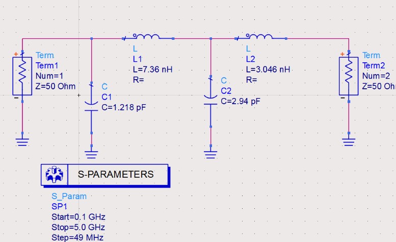
10. ADS Simulation Design Steps
Setup Workspace
Launch Keysight ADS, create a new workspace, and open a new schematic window.
Lumped Component Placement
Select L and C from the Lumped-Components library. Arrange components according to low-pass topology.
Component Parameterization
Enter calculated values: \(C_1=1.218\text{pF}\), \(L_2=7.35\text{nH}\), \(C_3=2.94\text{pF}\), \(L_4=3.046\text{nH}\).
Simulation & Verification
Perform S-parameter simulation to observe attenuation and verify that requirements are met.
Microwave Schematic Reference Fig

